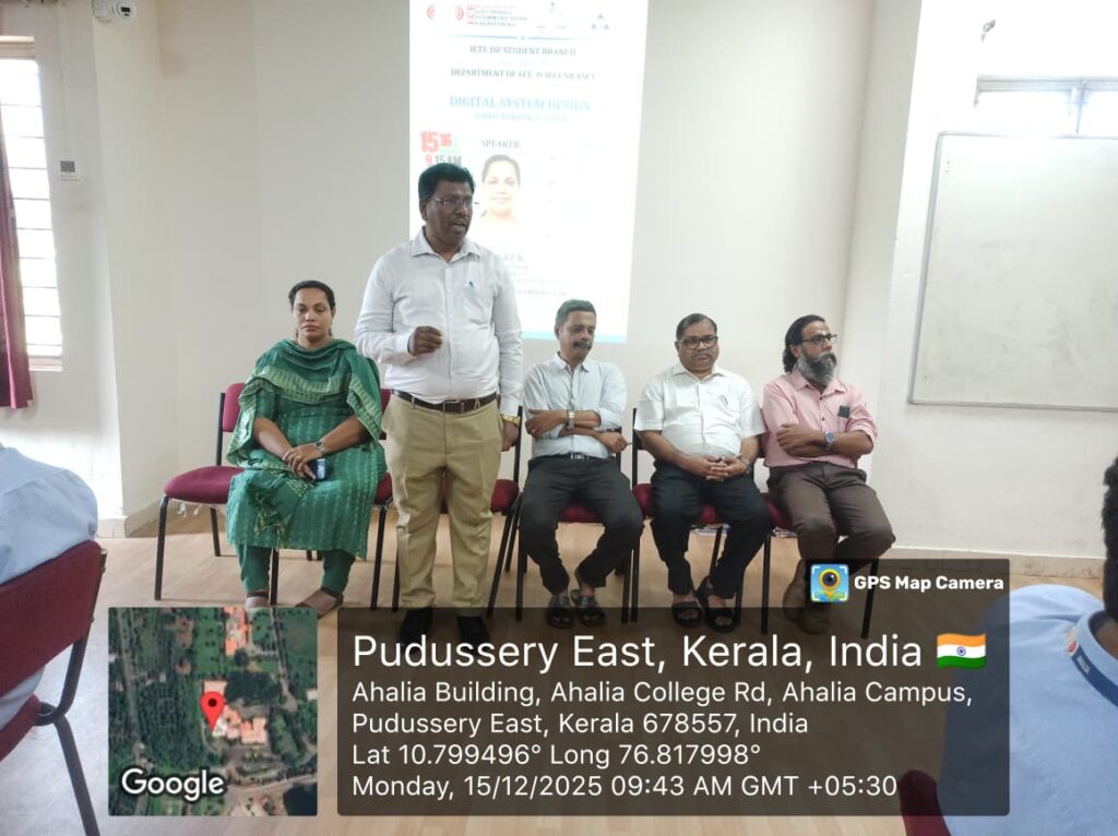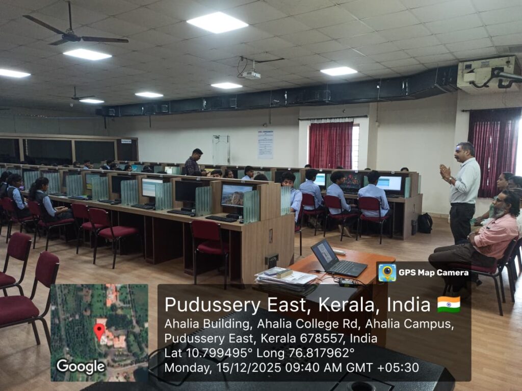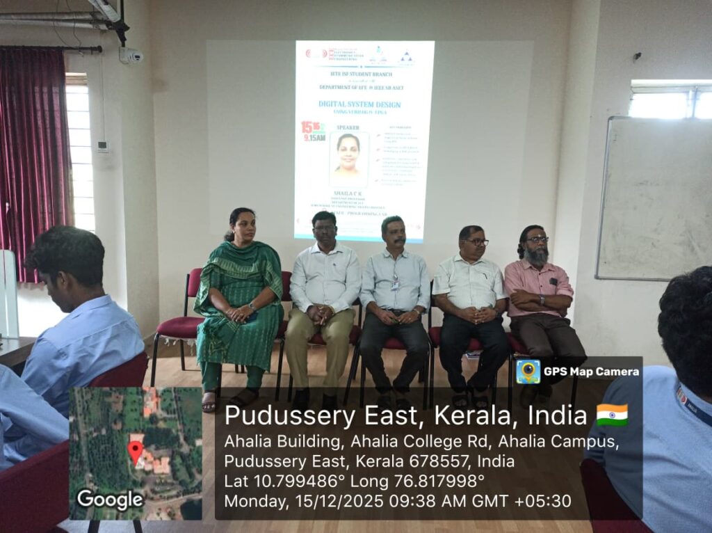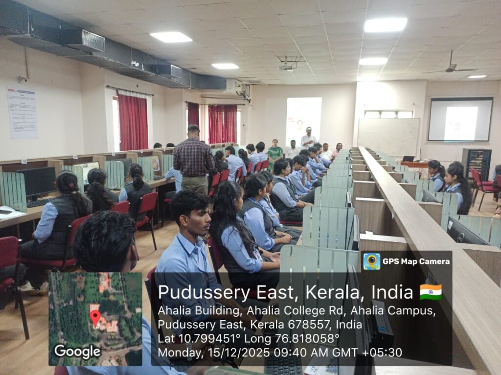
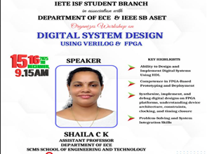
A two-day hands-on workshop on “Digital System Design using Verilog and FPGA” was organized with the objective of providing practical exposure to HDL-based digital design and FPGA implementation. The programme focused on bridging the gap between theoretical concepts and real-time hardware realization through structured lectures and extensive hands-on sessions. The workshop enabled participants to understand the complete digital design flow, from HDL coding to FPGA deployment.
| Item | Details |
| Title of the Programme | Two-Day Hands-on Workshop on Digital System Design using Verilog and FPGA |
| Type of Programme | Technical Hands-on Workshop |
| Dates | 15th & 16th December 2025 |
| Duration | Two Days |
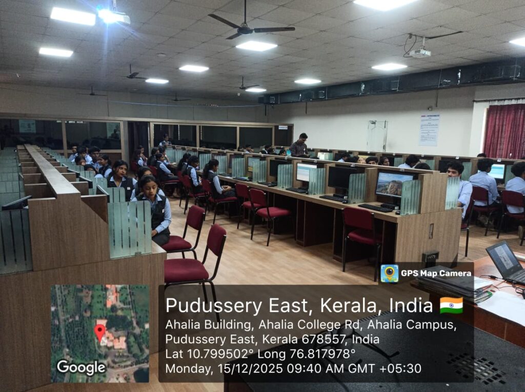
| Venue | Programming Lab 3 |
| Organised By | IETE–ISF Student Chapter |
| In Association With | Department of Electronics and Communication Engineering & IEEE Student Branch, Ahalia |
| Coordinator | Dr. Aneesh K – Dept of ECE |
| Resource Person | Ms. Shaila C K |
| Affiliation | Assistant Professor, Department of ECE, SCMS School of Engineering and Technology, Cochin |
| Target Participants | Undergraduate students of Electronics and Communication Engineering |
| Objectives of the Workshop | • To introduce HDL-based digital system design using Verilog • To provide hands-on exposure to FPGA-based implementation • To enhance understanding of synthesis, timing, and hardware debugging |
| Topics Covered | • Digital system design flow • Verilog HDL fundamentals and RTL coding • Combinational and sequential circuit design • FPGA architecture • Synthesis, implementation, and bitstream generation • Clocking, timing, and architectural constraints • Debugging on FPGA platforms |
| Tools / Platforms Used | Verilog HDL and FPGA design tools |
| Key Outcomes | • Ability to design and implement digital systems using HDL • Competence in FPGA-based prototyping • Skills in synthesis, implementation, and debugging on FPGA platforms • Understanding of architectural constraints, clocking, and timing analysis |
| Overall Impact | The workshop enhanced students’ practical skills in digital system design and FPGA implementation, preparing them for industry-oriented projects and advanced academic work. |
| Participants | 4th Semester Electronics and Communication Engineering Students |
| Number of Participants | 53 Students |
Feedback analysis:
The feedback received for the two-day workshop on Digital System Design Using Verilog and FPGA was highly positive. Most participants rated the workshop as very good to excellent, appreciating the clear explanation of objectives, relevance of the topics, and the strong subject knowledge of the resource person. Students reported noticeable improvement in their understanding of Verilog HDL and FPGA-based digital system design. The workshop was well organized and highly recommended by the participants, with a few suggestions for incorporating more hands-on practice and problem-solving sessions in future programs.